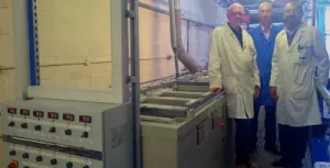
Always improving our systems and factory we've invested in a...
Read MoreBlog
Olympus SZX12 / DP50 microscope acquisition
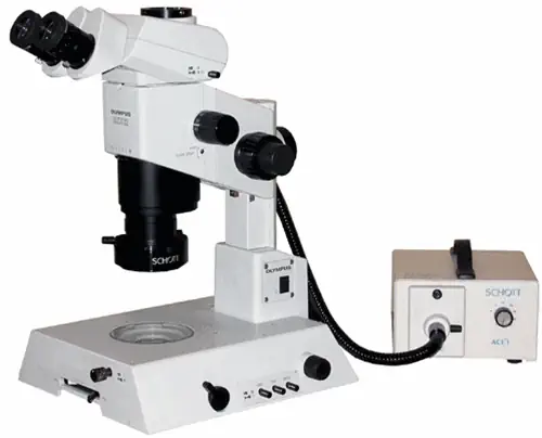
P.W. Circuits have invested in a new Olympus SZX12 / DP50 microscope with Olympus DP50 5.8 million pixels camera allowing even more detailed microsection analysis.
What is a microsection?
A PCB microsection is a cross-sectional view of a printed circuit board (PCB). It’s created by cutting a thin slice of the PCB and preparing it for microscopic examination. This destructive testing method is crucial for quality control and failure analysis in the PCB manufacturing industry.
Why is it done?
Microsections provide detailed information about the internal structure of a PCB, including:
- Plated through-hole (PTH) quality: Examining the copper plating thickness, adhesion, and overall integrity of PTHs.
- Layer thickness and registration: Checking the accuracy of copper layer thickness and alignment between layers.
- Solder mask coverage: Assessing the completeness and adhesion of the solder mask.
- Surface finish thickness: Measuring the thickness of various surface finishes (e.g., gold, nickel, tin).
- Material defects: Identifying voids, delaminations, or other defects within the PCB.
Failure analysis: Investigating the root cause of PCB failures by examining the internal structure.
By revealing the internal details of a PCB, microsection analysis helps ensure product quality, troubleshoot manufacturing issues, and understand the mechanisms of PCB failures.
We are constantly adding to our factory inventory in order to produce your quality PCBs.
This also means we can carry detailed specific checks an produce even more accurate reports according to your IPC Class 3 requirements.
Contact us today for more information on IPC classes or just general UK PCB manufacture.