Does Made in the UK really mean that or just...
Read MoreHalf a hole
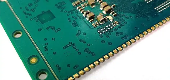
Half plated / castellated Technology. Half a hole PCB design

PW Circuits can now produce burr free half a hole PCB design, also know as castellated PCBs. Old methods of routing away half the hole resulted in a burr remaining or the plating being ripped out of the hole, but with new processing stages this can now be achieved.
Half holes, also known as castellated holes, are a type of through-hole that extends only partially through a PCB.
Unlike traditional through-holes that go completely through the board, Half a hole PCB design provide a plated surface on one side of the PCB for soldering components.
How do they work?
- Structure: Half holes are essentially plated through-holes cut in half. They have a plated wall on one side of the PCB, which acts as a landing pad for components.
- Function: Primarily used for board-on-board connections, half holes allow for the direct soldering of one PCB to another without the need for additional connectors. This provides a slimmer profile and potentially better electrical connection.
- Applications: Common applications include:
- Board-on-board connections: Combining different PCB technologies or adding modules.
- Fine-pitch SMD components: Providing a better landing pad for small components.
- RF assemblies: Used in high-frequency applications due to their reduced height.
Advantages of Half Holes
- Space-saving: Reduces overall PCB thickness.
Improved electrical connection: Direct soldering can provide better conductivity. - Cost-effective: Can eliminate the need for additional connectors.
- Enhanced reliability: Can reduce the risk of connection failures.
Contact us today for more information on your half hole PCBs.
Other PCB news blogs you might be interested in...
Olympus szx12 / dp50
Olympus SZX12 / DP50 microscope acquisition P.W. Circuits have invested...
Read More

