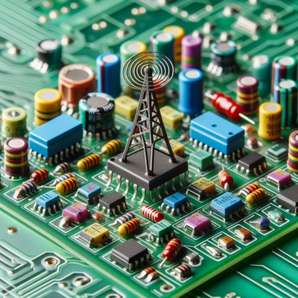
Microwave and Radio Frequency PCBs
The industry has seen an increase in the number of Microwave and Radio Frequency PCBs being manufactured at our Leicester site over the last few years. Including quadrafillar helix antenna & conformal patch antennas the range is now vast.
Characteristics of Microwave and Radio Frequency PCBs
Microwave and RF PCBs differ from conventional PCBs in several key aspects:
- Loss Tangent (tan δ): This parameter measures the amount of energy lost as the signal travels through the PCB. Lower tan δ values indicate better signal transmission, making it essential for microwave and RF applications.
- Dielectric Constant (εr): This property represents the ability of the PCB material to store electrical energy. A higher εr value can enhance signal propagation, but it can also lead to higher losses. Balancing εr and tan δ is crucial for optimizing RF performance.
- Return Loss (S11): This parameter measures the amount of signal reflected back to the source. Low return loss indicates efficient signal transmission, minimizing the loss of information.
With over 50 years of experience in the PCB industry, this wealth of knowledge has helped us push forward and become one of the top manufacturing specialists in this complex and demanding industry.
With manufacturing capabilities for single-sided, double sided plated through holes and Multilayer’s with mixed material builds, our expertise in manufacturing printed circuit boards with different complexities and demands over a wide range of sizes from 2 millimetres to over 2 Metres.
We hold stock of a wide range of microwave & RF materials meaning the once industry-standard of long lead times are now a thing of the past, visit our materials page for more information or contact a member of our sales team.
Please checkout our YouTube channel for more PCB manufacturing and design tips that could help you save time and money.