Flexi & flexi-rigid PCBs
Flexi and flexi-rigid PCBs are replacing traditional FR4 in a wide range of applications, offering benefits such as solving interconnection problems, reducing weight and space, and lowering assembly costs. Flexible applications can be either dynamic flexing (designed to flex or withstand stress over time at elevated temperatures) or flex and stay applications (designed to flex once and then be secured in place).
Standard flexi PCBs
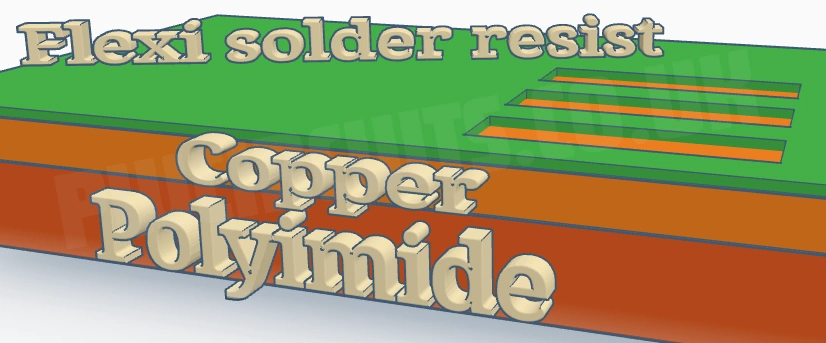
Single-sided flexible circuits are the most cost-effective solution for compact electronic designs. As the most straightforward flexible printed circuit (FPC) option, they feature a single conductor layer bonded to a thin, flexible dielectric film.
To ensure long-term durability and environmental protection, these circuits can be finished with a protective cover-lay or a flexible solder resist, making them ideal for “flex-and-stay” applications. For designs requiring local stability, you can integrate mechanical stiffeners to provide rigidity in specific areas, such as component mounting zones.
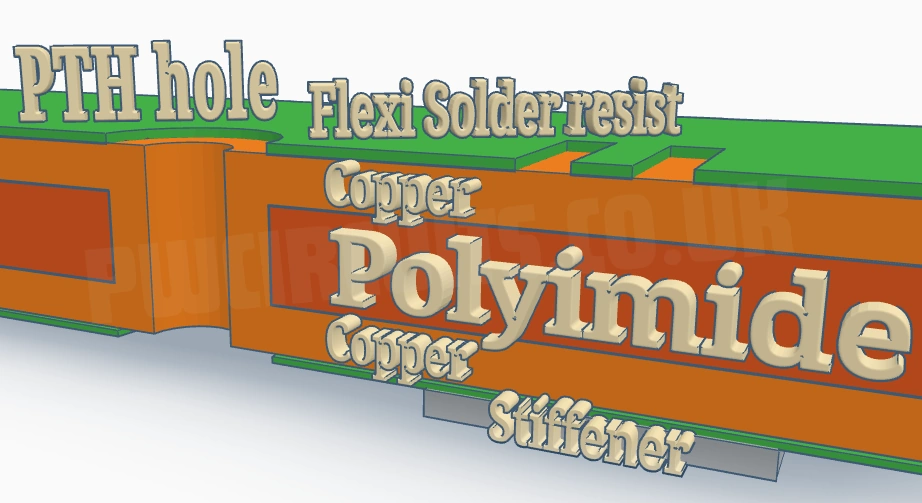
Double-sided flexible circuits (Type 2 per IPC-6013 standards) feature two conductive copper layers separated by a high-performance dielectric film, such as polyimide. This design significantly increases circuit density and allows for more complex routing compared to single-sided options.
To enable electrical communication between the layers, plated-through holes (PTH) or vias are integrated into the design. These circuits can be finished with a protective cover-lay or flexible solder resist to safeguard against environmental damage. For designs requiring structural reinforcement, mechanical stiffeners can be strategically added to support heavy components or protect fragile solder joints.
Advanced flexi & flexi-rigid PCBs
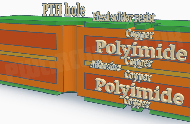
Multilayer flexible circuits are the most complex type of flexible printed circuit board (FPCB) design, offering three or more conductive copper layers separated by insulating dielectric films. This advanced structure is necessary for high-density interconnects (HDI) and complex electronic devices where board space is at a premium.
Interlayer connectivity is achieved through reliable plated-through holes (PTH), or vias, which route signals across multiple circuit planes. These robust circuits can be finished with a protective cover-lay or flexible solder resist for environmental durability. Structural integrity can be customised using mechanical stiffeners, allowing for rigid component areas alongside flexible sections tailored for dynamic bending.
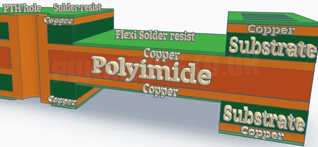
Rigid-flex PCBs represent the pinnacle of interconnect technology, seamlessly integrating flexible copper conductor layers on dielectric films with traditional rigid circuit board materials. This hybrid construction eliminates the need for bulky connectors and ribbon cables, significantly increasing reliability and reducing the overall weight of the assembly.
To ensure seamless electrical communication across the board, plated-through holes (PTH) are used to bridge the flexible and rigid sections. The flexible layers are protected by high-durability coverlays or flexible solder resists for dynamic movement. Standard solder mask is applied to the rigid zones for component soldering. This versatile design is the preferred choice for space-constrained, high-vibration environments like aerospace and medical electronics.
Flexi and flexi-rigid PCB guidelines and material specifications
Tie downs and teardrops
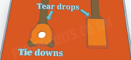
Through-holes in flexible circuits should be reinforced with tie downs. Tie downs are additional copper areas bonded to the pad that are secured by the coverlay to anchor the copper pad and prevent delamination between the copper and the base material. The adhesion of copper to flexible material is weaker than that of standard rigid material. Extra care must be taken when soldering flexible circuits.
Teardrops are the gradual transition from copper track to copper pad. This feature should be added to both through-hole pads and surface mount pads to reduce stress points and help eliminate breakage during flexing.
Coverlay options
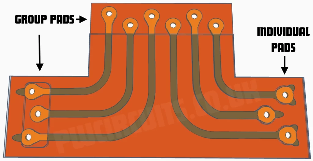
Coverlay is a flexible material applied to the outer layers of flexi and flexi-rigid PCBs to insulate the copper. It is typically made of polyimide or polyester. The coverlay is created using a drilling or routing process, which limits the shapes of openings. The simplest and most cost-effective method is to have individual pads, space permitting. A minimum of 0.20mm distance is required between individual pads. If space is limited, grouping pads is an option. The coverlay pad should be at least 0.25mm larger than the copper pad.
Coverlay around surface mount pads can be routed, but a radius will remain due to the size of the router. Alternatively, a laser cutting process can be used to reduce the radius. Semi-flexible solder resist (for some flex-and-stay applications) can be applied instead of a coverlay. This allows for any shape to be used with a minimum of 0.10mm distance between individual pads.
Flexi and flexi-rigid PCBs: staggered conductors
Staggering conductors (copper tracks) is recommended to preserve the circuits’ maximum flexibility.
“I beam” designs, where conductors on both layers are positioned directly on top of each other, should be avoided as they increase the stiffness of the circuits’ fold areas.
Fold Lines and Bend Radius
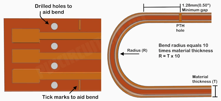
Fold lines can be incorporated into your design using tick marks, which can be added to either the copper layers or silkscreen layers. These ticks facilitate bending your flexi PCB in a specific location. The bend radius of your flexible circuit should be approximately 10 times the total material thickness, including copper.
A minimum gap of 1.28mm should be maintained between any plated-through holes. Tracks should be radiused to help mitigate breakage during folding and bending. The track widths should not be altered in the bend areas.
Copper Shielding
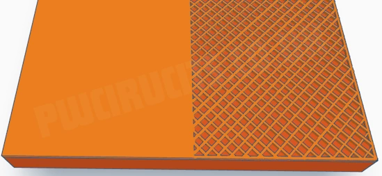
Solid copper shielding is the most widely used method but does increase the rigidity of the flexible circuit. It should be factored into the thickness-to-bend radius calculation. Crosshatched copper shielding helps to maintain the circuit’s flexibility. Copper shielding can cover all or selective areas on one or both sides.
Solid copper shielding provides excellent EMI/RFI protection but can make the circuit less flexible. Cross hatched copper shielding offers a compromise between shielding effectiveness and flexibility. The amount of shielding coverage can be tailored to specific areas of the circuit based on EMI/RFI considerations.
Flexi Stiffeners
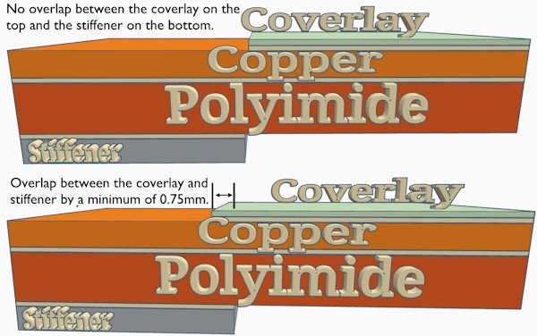
Additional support is often required in areas where connectors or components are mounted. Various materials can be employed as stiffeners, with FR4, polyimide, and polyester being the most common choices. Stiffener thicknesses range from 0.050mm to 2.400mm.
Bonding of stiffeners can be achieved using high-temperature pressure-sensitive tape or thermal setting adhesive. Holes in stiffeners should be 0.40mm larger than the corresponding holes in the flexible circuit to facilitate registration. To eliminate potential stress points and cracking, the stiffener should overlap the coverlay by at least 0.75mm.
Base Materials for flexi and flexi-rigid PCBs
A variety of copper thicknesses are available for the base material, including 5, 9, 18, 35, 70, and 105 microns, and they can be applied to one or both sides. The polyimide substrate is available in thicknesses of 12, 25, 50, 75, and 125 microns, with 25 and 50 microns being the standard thicknesses. Coverlay polyimide thickness options include 12, 25, 50, 75, and 125 microns, with 25 and 50 microns being the standard thicknesses. Adhesive thicknesses are available in 12, 25, and 50 microns. FR4 and polyimide stiffeners start at 0.050mm thickness. For more information visit our flexi materials page.
Contact us today so we can quote all you for your flexi and flexi-rigid PCBs needs. Why don’t you check out our YouTube channel for more design hints.