About the PCB
The history of the Printed Circuit Board
The PCB is used to connect electrical components via conductive tracks and pads that have been etched away from a sheet of copper. Before the existence of the printed circuit board, point to point construction was bulky and unreliable. These designs required regular maintenance and replacement. The predecessor, ECME, worked by spraying metal onto a board of plastic allowing it to make 3 radios per minute. Since then the PCB has become the common component used in electronics.
Initially, the PCB had holes drilled so that wire leads could be passed through and soldered. This was known as through-hole construction. Then in 1949, the auto assembly process was invented whereby wire leads were inserted into a copper foil interconnection pattern. Finally, in 1980, the old style of through-hole wire leads was largely replaced with plating down the holes. The use of smaller surface mount parts resulted in smaller and less costly boards too.

Manufacture of the Printed Circuit Board
Once a customer has produced a design, they export their design into the format that is used by their manufacturer. The most popular format, and the one used at PW Circuits, is the Gerber format. Before the file is exported, the design is checked by the software for any errors. The generation of Gerber files will encode important information including copper tracking, apertures, component notations and other options.
When PW Circuits receives the files, we run a Design for Manufacture check to ensure that the design meets minimum tolerances. After this, we print the design a “photoplotter”, which uses a light source to carefully and intricately draw the various tracks onto high-contrast photographic film. The result can’t yet be seen, however, as it has to be developed with another machine that uses a developer solution.
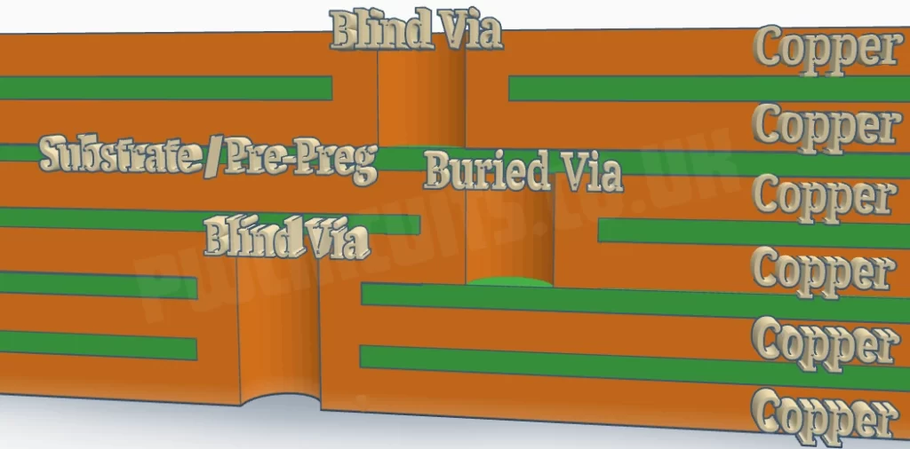
Using the newly created plots, we can now cover the appropriate areas with photo resist, which involves using UV light to protect any of the areas based on whether they are clear or black, and then use a chemical solution to remove copper that is not covered with photo resist. The result, after removing the still remaining photo resist is the base material with intricate copper tracks running along it. Now all the layers must be carefully aligned and combined using prepreg. The only remaining stage is to drill the board in preparation for components. Holes are drilled as small as 100 microns, thinner than a hair.
Visit our YouTube Channel for more details and help when designing PCBs.
Why are PCBs green?
There isn’t an extremely important reason for the colour of the PCB. In actual fact, many varying colours of solder mask are available but there are still good reasons for the use of green:
- Green is both facile for the eye to look at and easier for inspection. At this perfect balance technicians will have a better time looking for errors in the PCB
- Because everyone uses green, the colour is widely produced in large quantities which reduces the cost of the PCB
- Most research into improving solder mask has gone into the green version, this means that the green solder mask now has a better performance than other colours.
Multilayer PCB World Record
As technology advances, more and more amazing attributes can be added to the Printed Circuit Board. Features such as flexible boards / materials, ceramic base PCBs, radio frequency boards and multilayer are just a few examples of the constant expansion achieved in the PCB industry. At PW Circuits, up to 32 layers can be combined in a multilayer PCB but the current world record is a manufacturer in Japan, who produced 129 layers in a single PCB.
