Controlled Impedance
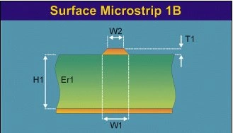
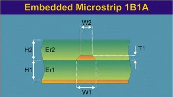
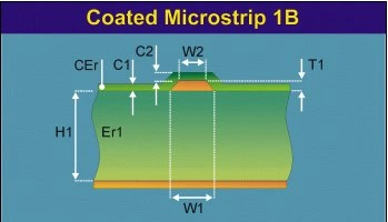
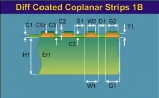
Designers and fabricators work together to control the characteristic impedance of PCB transmission lines in controlled impedance PCBs. This helps ensure high signal integrity across a wide range of applications.
Impedance is measured in Ohms (Ω) and is an AC characteristic which becomes important as the signal frequency increases. Typically they become critical for PCB traces at signal components of two hundred MHz and above.
Our trained CAD engineers are more than happy to work with you at your design stage on any of your controlled impedance PCBs. Multiple impedance requirements can be added to one board. Ranging from a single track on a surface layer to multiple impedance buried deep in multilayers.
We offer a two-step verification process for your controlled impedance PCBs:
Design Review: Our licensed Polar software allows our engineers to directly verify your track widths, gaps, layer stackup, and impedance calculations. This ensures your design meets your specifications and is manufacturable.
Impedance Testing: During PCB manufacturing, we include additional impedance coupons on the panels. These coupons mirror your exact track and gap requirements. After fabrication, we use our Polar CITS Impedance software and hardware to test these coupons, confirming that the manufactured impedance matches your design calculations.
Get a complete picture of your controlled impedance PCB project: We can include a detailed impedance test report with your delivered boards. Simply request this option during the quotation process to ensure you receive it.
Use one of our multiple impedance calculators available on our website. Choose from the menu above.


For further details on any of the above, don’t hesitate to contact a member of our team.