Multilayer PCB manufacture
Multi layer PCBs
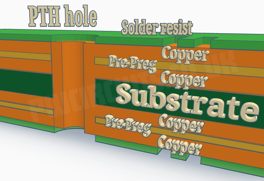
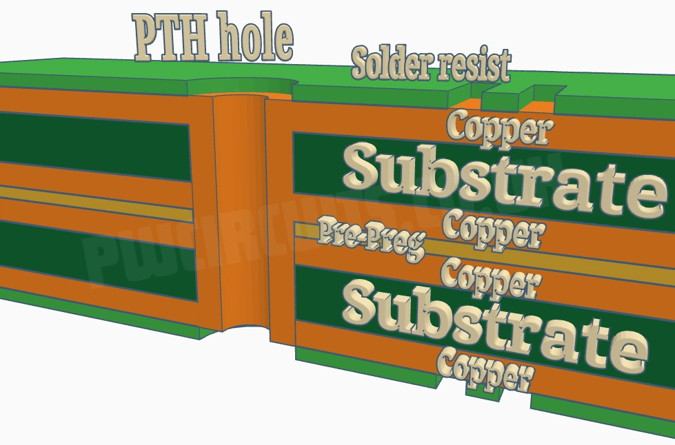
Multilayer PCBs consist of three or more conductive copper layers sandwiched between insulating substrates (Pre-preg (usually made of epoxy resin or fiberglass)). The layers are interconnected through vias—tiny holes drilled through the board—allowing signals to flow between different layers. Each layer serves a specific purpose: signal routing, power distribution, and ground planes. The outer layers (top and bottom) typically handle signal traces, while inner layers manage power and ground connections.
P.W. Circuits have multilayer approval BS123300-003 up to a maximum of 32 layers!
Advantages:
- Higher Density: Multilayer boards accommodate a large number of components, making them ideal for densely populated electronic systems.
- Signal Integrity: With multiple layers, designers can route signals efficiently, minimizing interference and ensuring reliable communication.
- Thermal Management: The additional layers enhance heat dissipation, crucial for high-power applications like CPUs and power amplifiers.
- Reduced Electromagnetic Interference (EMI): Properly designed multilayer PCBs minimize EMI by separating sensitive analog signals from noisy digital traces.
- Compact Form Factor: Multilayer boards allow complex circuits to fit within smaller dimensions, critical for portable devices.
Via / Micro Vias
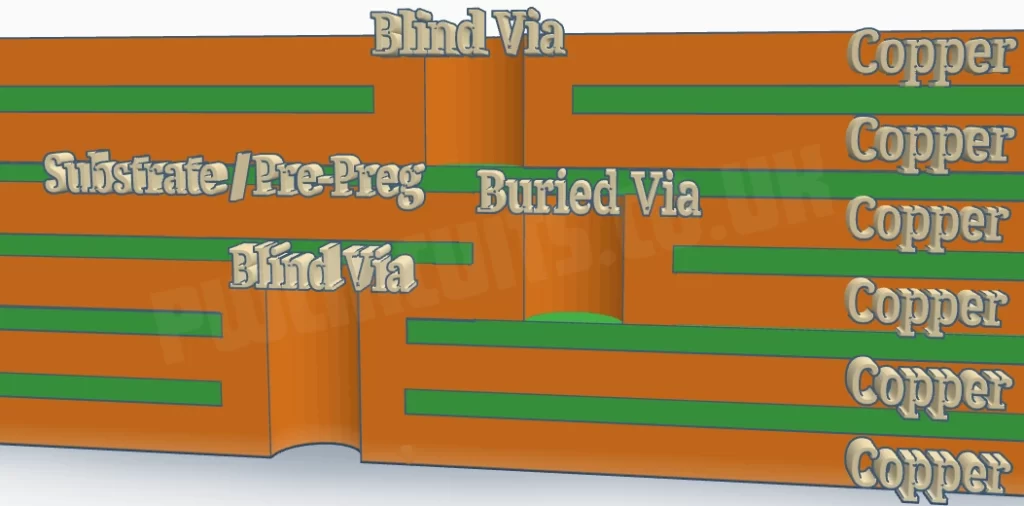
Micro via’s are connecting holes through the whole board. When there are multiple layers of conductor patterns and you only require some of them to be connected, buried & blind via’s can be used. Buried via’s connect inner layers together but not to the surface layers,. Blind via’s connect one of the surface layers to one or more of the inner layers.
Materials
There is a huge range of materials available for both single and multilayer printed circuit boards. We have an extensive list of substrate manufacturers and their data sheets.
Material search tool
As mentioned, the amount of substrates available is vast. Not sure what you require. Perhaps you are trying to source an alternative material. Or you just want to know what's available on the market? Our material search tool will help you streamline the available options.
Impedance Calculations
Our site had multiple impedance calculators to help you work out what substrates and thickness etc. you will require in order to achieve your desired results.
You can submit your multi-layer Gerber (or DXF) files on our online quoting page to get a fast quote back.
Don’t forget to checkout and subscribe to our YouTube Channel. With informative video’s on how to get the best out your boards, money saving tips and design hints it’s a great a always growing source of information.